


My new Lumia is a pretty fancy phone, but its battery could be better. I wanted to make a DC to DC switching regulator, so that I could recharge my phone with an external battery during the hiking trips. If you are like me and don’t want to buy a ready made product, read further ¤Öé If someone wonders, why I’m not hunting ducks, the reason is that I wetted my boots and now my nose is little stuffy. Gladly, I took my “lab” with me since I designed to spend the daytime at the place of family friends, but now I’m still making this update comfortably inside. Such a rugged hunter ¤śĆ
As a disclaimer, I don’t take any responsibility about the possible damages these instructions result and I don’t guarantee the proper functioning of the device, like described in the About the Site page.
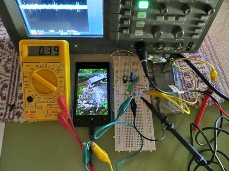
Some cell phones, like the Lumia 520, can be recharged via USB. USB ports give 5 volts and the maximum current of USB 2.0 is 500 mA, at least I have understood so. Thus, I started this project by checking how clean is the voltage given by the USB. One laptop’s USB had approximately 40 mVpp AC component without a load, which is pretty much if you ask me. I took this for my reference that I should beat. I also noticed that my Lumia didn’t take the maximum 500 mA, even if the battery was empty.
The easiest way to make 5 volts out of higher voltages is to use a linear DC-DC regulator, but their energy economy is poor since they waste all the excess power as heat. The switching regulators, like the 5 volt LM2574 I used, cuts the input voltage so that after filtering it by LC low-pass filters the load sees steady, down regulated DC voltage. Though, the switching produces noise which could be a problem. Here is my final schematic I used.
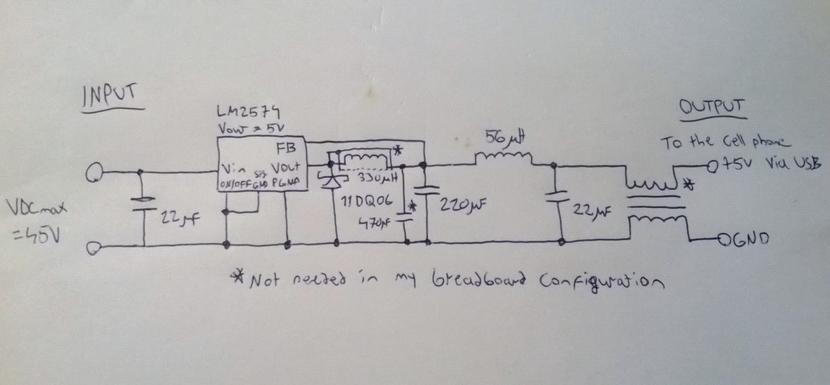
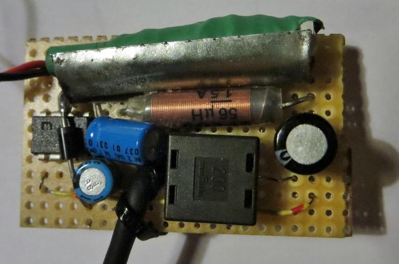
Most of the circuit is copied from the LM2574 datasheet, but I added extra components for cleaning the output voltage. The first wiring on the breadboard worked with less components since the connection I made was spacious. Thus, internally produced noise wasn’t a problem. For example, the magnetic fluxes from the first inductor didn’t much reach the second filtering inductor which was placed almost perpendicular to the first one. But in the final, more compact circuit I put the two inductors close and anti-parallel to each other. This is a really bad practice. The magnetic fluxes had a lot of common surface area for jumping from the first inductor to the second one and carry the switching noise further along the connection. That’s why I placed a thin, bended metal sheet between the inductors and connected it to the base of the first inductor. Now the noise has a good pathway to return back to its origin. I didn’t see any difference if the shield was connected to the inductor’s base or straightly to the ground. Without the shield the noise increased approximately 10 mVpp.
In the final circuit I added the small 470 pF ceramic capacitor parallel after the first inductor for guiding high frequency noise in the ground. Ceramic capacitors are faster than electrolyte capacitors, why they are better for handling high frequency noise. The recommended size of the first actual output capacitor is 22 uF, but I increased this to 220 uF. The second inductor capacitor pair forms the second LC low-pass filter. The cutoff frequency, where the attenuation is -3 dB, is calculated by the formula: f = 1/(2pi((LC)^(1/2))). Thus, the second LC filter attenuates 4.5 Hz by -3 dB and higher frequencies even more. This is much lesser than the switching frequency of the regulator. Though, parasitic capacitance and inductance may, or better will, produce unwanted resonance, why different arrangements and components are needed to try in practice for polishing the output voltage.
It┬Āis good to keep the wires between the ground and the Schottky diode, the first 22 uF capacitor and the capacitor after the first inductor as short as possible, for decreasing the reach of the switching noise. It is also good to connect the signal ground to downstream relative to the load. That’s because wires always have parasitic resistance which produces voltage difference when current is applied. Thus, if the signal ground is attached further from the main ground than the load ground, the relatively heavy and changing load currents will vary the potential the signal ground sees.
I coiled the first 330 uH inductor by myself, because I didn’t find any without ordering. First I checked that the copper wire can conduct at least 1 A without any problems and then I coiled it around the ferrite bar. I used an inductance meter for measuring the appropriate amount of turns. When I got the 330 uH I finished the coiling and sealed the inductor.
Whit a dummy┬Ā420 mA resistor load the output ripple was about 24 mVpp. Good! If the Lumia was recharged with lesser 380 mA current, the output ripple was approximately 60 mVpp. Thus, it looks like the phone injected some noise in my circuit. Sometimes much stronger, clearly digital distortions were seen while recharging. If the voltage in the external battery went too low, the phone started to cut the recharging on and off, a good sign for recharging the external battery. So, if you give maximally 45 VDC to this circuit, it should recharge any USB compatible device attached to it ¤Öé